7 minutes
Glasgow Interface Explorer - Reading SPI Flash Memory
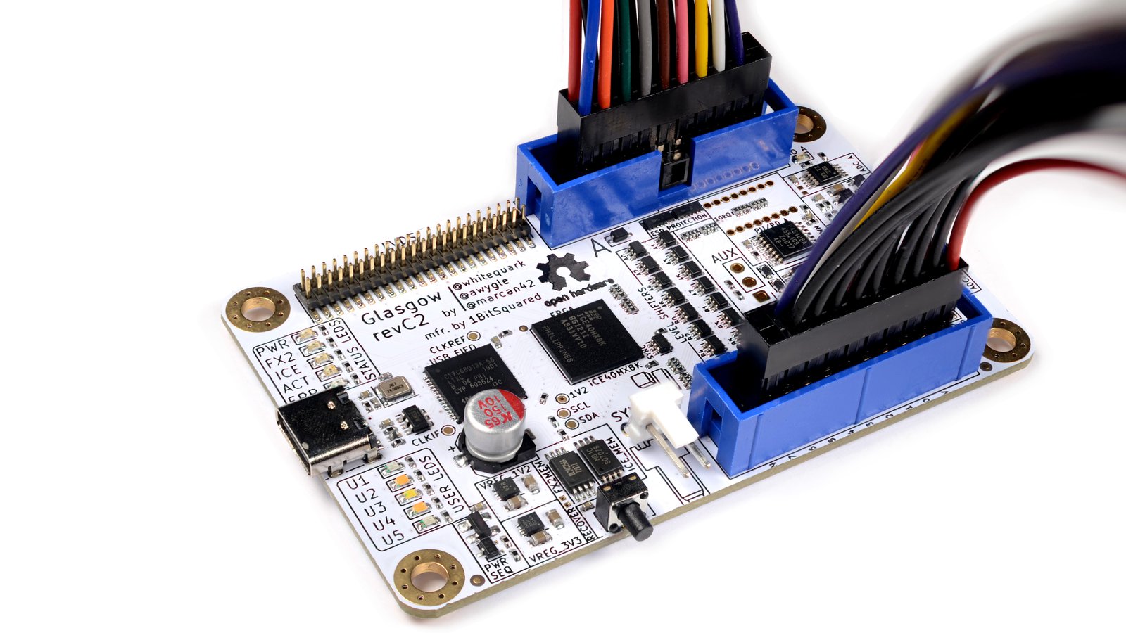
Glasgow Interface Explorer
The Glasgow Interface Explorer is self-described as a tool for exploring digital interfaces, aimed at embedded developers, reverse engineers, digital archivists, electronics hobbyists, and everyone else who wants to communicate to a wide selection of digital devices with high reliability and minimum hassle.
The device is capable of communicating with standard protocols including UART, SPI, and I2C, as well as reading and writing memory chips, programming microcontrollers, and much, much more. The Glasgow stands out amongst other hardware hacking tools because it uses reconfigurable logic, via an iCE40 FPGA, to communicate with devices - you can program the Glasgow on the fly to adapt to custom or obsolete interfaces.
It’s a seriously cool piece of hardware which you can pre-order on crowdsupply.
SPI Flash Memory
SPI is a synchronous serial communication interface. It’s used for communicating between a single controller (in this case a Glasgow) and one or more peripheral devices (the SPI flash chip). It’s a full-duplex interface meaning it supports bilateral communication between the controller and peripheral via the two data lines.
Flash memory is a non-volatile memory storage medium for embedded devices. You’ll find it storing device firmware, program data, so on.
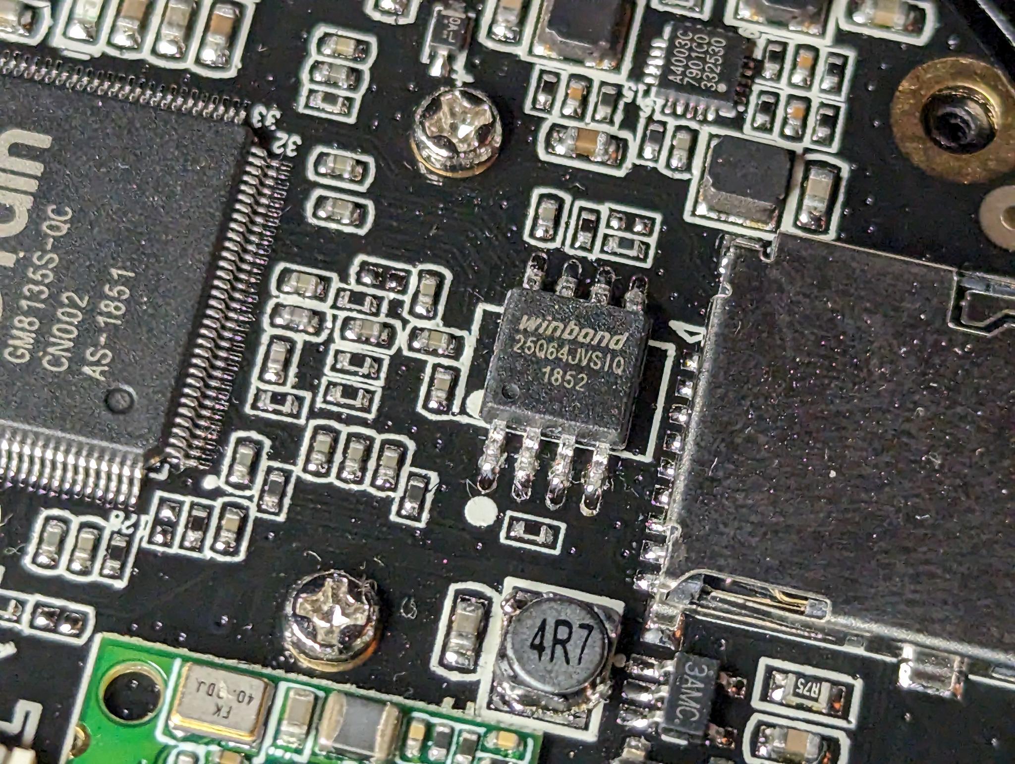
We’re going to look at a winbond W25Q64JV. It’s a 64Mb chip released in ~2015 that costs about a dollar fifty. Why this chip? Because I found it in a janky IoT camera in box of fractally-janky IoT devices destined to emit blue smoke.
   ┌────────────────────────┐
┌──┴─┐                    ┌─┴──┐
│CS# │ 1 ██             8 │VCC │
└──┬─┘                    └─┬──┘
┌──┴─┐                    ┌─┴──┐
│CIPO│ 2                7 │HOLD│
└──┬─┘      W25Q64JV      └─┬──┘
┌──┴─┐                    ┌─┴──┐
│WP# │ 3                6 │SCK │
└──┬─┘                    └─┬──┘
┌──┴─┐                    ┌─┴──┐
│GND │ 4                5 │COPI│
└──┬─┘                    └─┬──┘
   └────────────────────────┘
The W25Q64JV pin assignments are displayed above. You can identify pin 1 because it’s next to the little notch or circular impression on the top of the chip.
I’m using a SOIC 8-pin test clip to connect to the W25Q64JV chip. Make sure the red line on the ribbon is placed over line 1 on the chip!
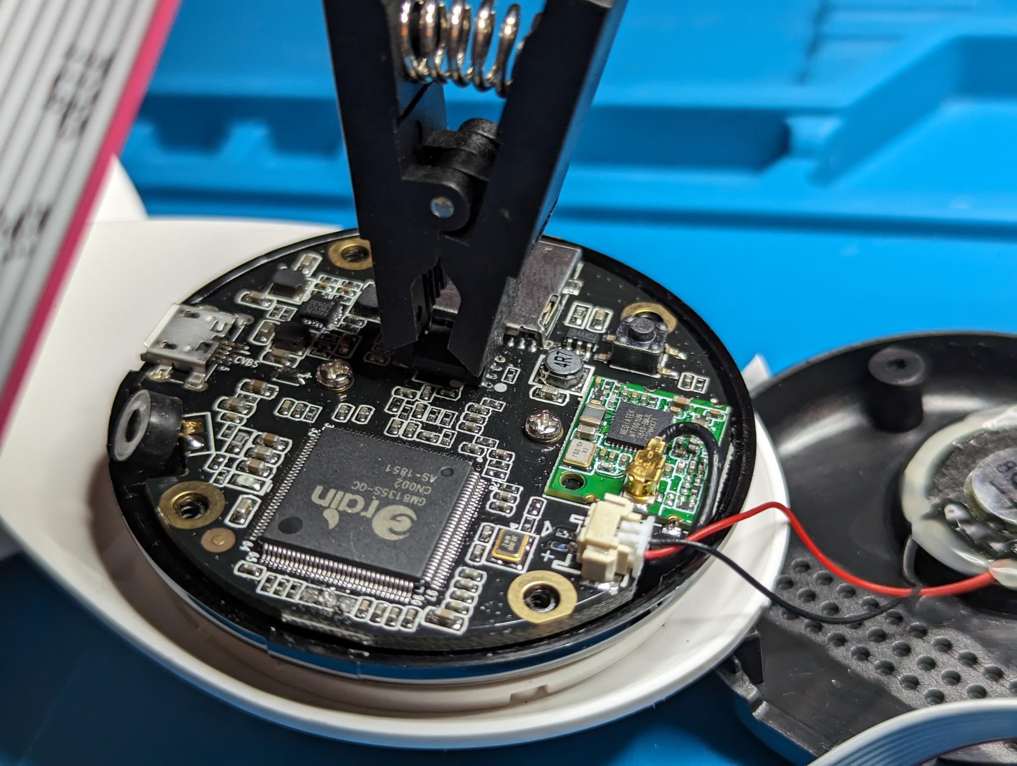
To read memory from this chip we’ll need to connect each line from it to the Glasgow.
If you’re following along on your own device, make sure that it’s not powered when connecting to the Glasgow. Since we’ll provide power from the Glasgow directly to the SPI chip via the VCC line a secondary power source from the IoT device may damage the chip or other components in the device.
Connecting the Glasgow
Look at Port A on the image below. It’s the upper 20-pin IDC connector. You’ll see 8 IO lines numbered 0 to 7 (coloured in orange). We’ll assign SPI lines to each of these I/O lines at run-time via command line arguments.
What exactly are we connecting? There are 4 important SPI lines you should to know:
CS: Chip Select
The controller uses this line to tell a peripheral that that data is being sent.
SCK: Serial Clock
The clock line is used to set the data transmission rate.
COPI: Controller Out, Peripheral In
The COPI line carries data from the controller to the peripheral.
CIPO: Controller In, Peripheral Out
The CIPO line carries data from the peripheral to the controller.
In addition to these 4 SPI lines, we’ll also need to power the chip via the VCC line, ground the chip via a GND line, and connect the WP# line (used for write protect input), and finally the HOLD line (used for Hold or Reset input).
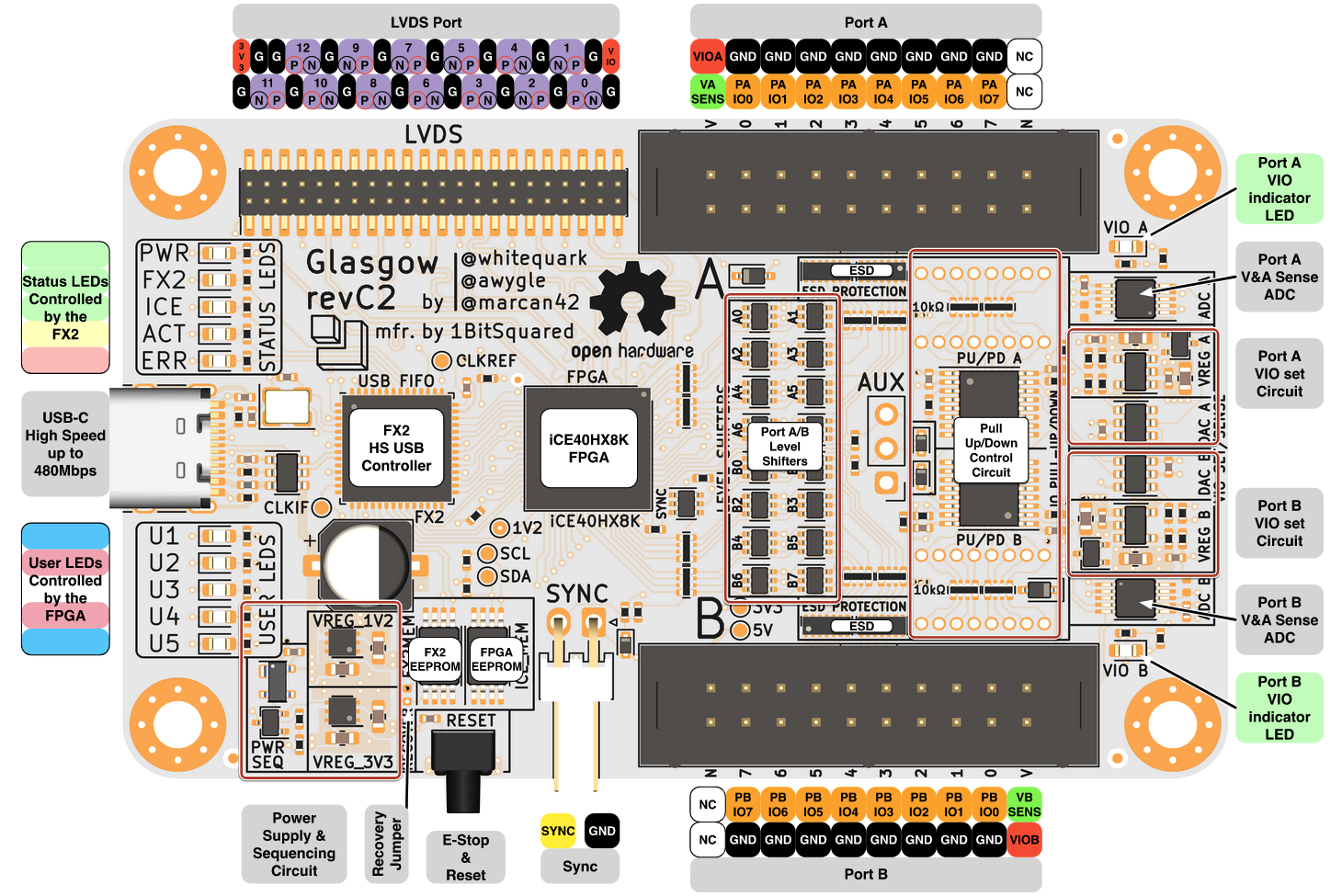
Image below shows how I’ve connected my chip to the Glasgow. You can connect your IO lines in any order but make sure that your chip is grounded and powered using the VIOA and GND lines on the Glasgow.
┌───────────────────────────────────────────────────────────────┐
│                              PORT A                           │
│ ┌────┐┌────┐┌────┐┌────┐┌────┐┌────┐┌────┐┌────┐┌────┐ ┌────┐ │
│ │VCC ││GND ││    ││    ││    ││    ││    ││    ││    │ │    │ │
│ └────┘└────┘└────┘└────┘└────┘└────┘└────┘└────┘└────┘ └────┘ │
│ ┌────┐┌────┐┌────┐┌────┐┌────┐┌────┐┌────┐┌────┐┌────┐ ┌────┐ │
│ │    ││CS# ││CIPO││COPI││SCK ││WP# ││HOLD││    ││    │ │    │ │
│ └────┘└────┘└────┘└────┘└────┘└────┘└────┘└────┘└────┘ └────┘ │
│   V     0     1     2     3     4     5     6     7      N    │
└───────────────────────────────────────────────────────────────┘
Glasgow
Glasgow CLI organizes core capabilities into applets. Each applet exposes functions such as reading or writing memory, determining JTAG pinout, and so on.
We’ll use the memory-25x applet because we’re working with a 25x chip. The memory-25x applet operations are listed below.
$ glasgow run memory-25x -h

<snip>

positional arguments:
  OPERATION
    identify                identify memory using REMS and RDID commands
    read                    read memory using READ command
    fast-read               read memory using FAST READ command
    program-page            program memory page using PAGE PROGRAM command
    program                 program a memory region using PAGE PROGRAM command
    erase-sector            erase memory using SECTOR ERASE command
    erase-block             erase memory using BLOCK ERASE command
    erase-chip              erase memory using CHIP ERASE command
    erase-program           modify a memory region using SECTOR ERASE and PAGE PROGRAM commands
    protect                 query and set block protection using READ/WRITE STATUS REGISTER commands
    verify                  read memory using READ command and verify contents

<snip>
Let’s examine the chip info to check it’s JEDEC ID and ensure the chip is actually a W25Q64JV. To do so we’ll use the identify operation in the memory-25x applet which will return the JEDEC ID and some other basic info about the chip.
Assign SPI lines to the Glasgow using the --pin-* positional arguments which should match the previous diagram if you’re following along. Use the -V positional argument to set the voltage for the chip. We’ll use 3.3V which we’ve already learned from the W25Q64JV datasheet.
$ glasgow run memory-25x -V 3.3 --pin-cs 0 --pin-cipo 1 --pin-copi 2 --pin-sck 3 \
--pin-wp 4 --pin-hold 5 identify

I: g.device.hardware: building bitstream ID 7d418322d63a0291d83cefa19b3b57c4
I: g.cli: running handler for applet 'memory-25x'
I: g.applet.memory.25x: port(s) A, B voltage set to 3.3 V
I: g.applet.memory.25x: JEDEC manufacturer 0xef (NEXCOM) device 0x16 (8-bit ID)
I: g.applet.memory.25x: JEDEC manufacturer 0xef (NEXCOM) device 0x4017 (16-bit ID)
I: g.applet.memory.25x: device has valid SFDP 1.5 (JESD216A) descriptor
I: g.applet.memory.25x:   SFDP table #0: JEDEC, Flash Parameter Table 1.5 (JESD216A)
I: g.applet.memory.25x:     density (Mebibits)     : 64
I: g.applet.memory.25x:     density (Mebibytes)    : 8
I: g.applet.memory.25x:     address byte count     : 3
I: g.applet.memory.25x:     write granularity      : 64 byte(s)
I: g.applet.memory.25x:     sector sizes           : 4096, 32768, 65536
I: g.applet.memory.25x:     sector size 4096       : erase opcode 0x20
I: g.applet.memory.25x:     sector size 32768      : erase opcode 0x52
I: g.applet.memory.25x:     sector size 65536      : erase opcode 0xd8
I: g.applet.memory.25x:     double transfer rate   : yes
I: g.applet.memory.25x:     fast read modes        : (1-1-2), (1-1-4), (1-2-2), (1-4-4), (4-4-4)
I: g.applet.memory.25x:     fast read mode (1-1-2) : opcode 0x3b, 8 wait states, 0 mode bits
I: g.applet.memory.25x:     fast read mode (1-1-4) : opcode 0x6b, 8 wait states, 0 mode bits
I: g.applet.memory.25x:     fast read mode (1-2-2) : opcode 0xbb, 2 wait states, 2 mode bits
I: g.applet.memory.25x:     fast read mode (1-4-4) : opcode 0xeb, 4 wait states, 2 mode bits
I: g.applet.memory.25x:     fast read mode (4-4-4) : opcode 0xeb, 0 wait states, 2 mode bits
Once we have this info we can use the datasheet to confirm that the JEDEC ID 0xEF is Winbond and the device ID 0x4017 is W25Q64JV-IQ/JQ.
Reading Flash Memory
We’ll read the chip using the fast-read operation, specifying an output filename using the -f positional arg, a start offset of 0, and the number of bytes to read, and then give it a few minutes to cook.
$ glasgow run memory-25x -V 3.3 --pin-cs 0 --pin-cipo 1 --pin-copi 2 --pin-sck 3 \
--pin-wp 4 --pin-hold 5 fast-read 0 8388608 -f firmware.bin

I: g.device.hardware: device already has bitstream ID 7d418322d63a0291d83cefa19b3b57c4
I: g.cli: running handler for applet 'memory-25x'
I: g.applet.memory.25x: port(s) A, B voltage set to 3.3 V
Then we’ll unblob the resulting binary file.
$ unblob firmware.bin

2023-07-13 02:06.20 [info     ] Start processing file          file=firmware.bin pid=34067
2023-07-13 02:06.20 [warning  ] Found unknown Chunks           chunks=[0x0-0x346f4, 0x21ec3a-0x220000, 0x530000-0x540000] pid=34071
2023-07-13 02:06.20 [info     ] Extracting unknown chunk       chunk=0x0-0x346f4 path=firmware.bin_extract/0-214772.unknown pid=34071

<snip>
Open the extracted squashfs filesystem.
$ cd firmware.bin_extract/2228224-5439488.squashfs_v4_le_extract
$ ls

bin  boot.sh  dev  etc  gm  home  init  lib  mnt  npc  opt  patch  proc  rom  root  sbin  share  squashfs_init  sys  tmp  usr  var
And poke around…
$ cat etc/issue


Welcome to \n (\m-\s-\r@\l/\b)
Grain Media ARM Linux 3.3

Copyright (C) 2005 Faraday Corp. <www.faraday.com.tw>
Released under GNU GPL